Texas Instruments offers a complete, broad portfolio of products, including registers, buffers, switches, drivers, gates, comparators, flip flops, and voltage translation. TI linear and logic solutions deliver application flexibility, higher performance, and design longevity.
Little Logic
Little Logic devices from Texas Instruments (TI) are the pieces that help complete the design puzzle and win in today’s marketplace.
- Smaller pieces, faster time-to-market
- Many pieces, one-stop selection
- Every Piece, Every Time
- Better Pieces, customer centric
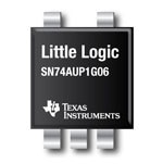
SN74AUP1G06DRYR
Low-Power Single Inverter Buffer/Driver with Open-Drain Outputs
Click for more information.
- Available in the Texas Instruments NanoStar™ Package
- Low Static-Power Consumption (ICC = 0.9 µA Max)
- Low Dynamic-Power Consumption (Cpd = 1 pF Typ at 3.3 V)
- Low Input Capacitance (Ci = 1.5 pF Typ)
- Low Noise – Overshoot and Undershoot <10% of VCC
- Ioff Supports Partial Power-Down-Mode Operation
- Input Hysteresis Allows Slow Input Transition and Better Switching Noise Immunity at the Input (Vhys = 250 mV Typ at 3.3 V)
- Wide Operating VCC Range of 0.8 V to 3.6 V
- Optimized for 3.3-V Operation
- 3.6-V I/O Tolerant to Support Mixed-Mode Signal Operation
- tpd = 3.6 ns Max at 3.3 V
- Suitable for Point-to-Point Applications
- Latch-Up Performance Exceeds 100 mA Per JESD 78, Class II
- ESD Performance Tested Per JESD 22
- 2000-V Human-Body Model (A114-B, Class II)
- 1000-V Charged-Device Model (C101)

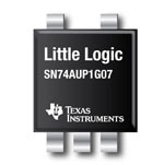
SN74AUP1G07DRYR
Low-Power Single Buffer/Driver with Open-Drain Outputs
Click for more information.
- Available in the Texas Instruments NanoStar™ Package
- Low Static-Power Consumption (ICC = 0.9 µ Maximum)
- Low Dynamic-Power Consumption (Cpd = 1 pF Typical at 3.3 V)
- Low Input Capacitance (Ci = 1.5 pF Typical)
- Low Noise – Overshoot and Undershoot <10% of VCC
- Ioff Supports Partial-Power-Down Mode Operation
- Input Hysteresis Allows Slow Input Transition and Better Switching Noise Immunity at the Input (Vhys = 250 mV Typ at 3.3 V)
- Wide Operating VCC Range of 0.8 V to 3.6 V
- Optimized for 3.3-V Operation
- 3.6-V I/O Tolerant to Support Mixed-Mode Signal Operation
- tpd = 3.3 ns Maximum at 3.3 V
- Suitable for Point-to-Point Applications
- Latch-Up Performance Exceeds 100 mA Per JESD 78, Class II
- ESD Performance Tested Per JESD 22
- 2000-V Human-Body Model (A114-B, Class II)
- 1000-V Charged-Device Model (C101)


SN74AUP1G80DRYR
Low-Power Single Postitive-Edge-Triggered D-Type Flip-Flop
Click for more information.
- Available in the Texas Instruments NanoStar™ Package
- Low Static-Power Consumption (ICC = 0.9 µA Max)
- Low Dynamic-Power Consumption (Cpd = 4.3 pF Typ at 3.3 V)
- Low Input Capacitance (Ci = 1.5 pF Typ)
- Low Noise – Overshoot and Undershoot <10% of VCC
- Ioff Supports Partial-Power-Down Mode Operation
- Schmitt-Trigger Action Allows Slow Input Transition and Better Switching Noise Immunity at the Input (Vhys = 250 mV Typ at 3.3 V)
- Wide Operating VCC Range of 0.8 V to 3.6 V
- Optimized for 3.3-V Operation
- 3.6-V I/O Tolerant to Support Mixed-Mode Signal Operation
- tpd = 4.4 ns Max at 3.3 V
- Suitable for Point-to-Point Applications
- Latch-Up Performance Exceeds 100 mA Per JESD 78, Class II
- ESD Performance Tested Per JESD 22
- 2000-V Human-Body Model (A114-B, Class II)
- 1000-V Charged-Device Model (C101)


SN74AUP1G00DSFR
Low-Power Single Two-Input Positive-NAND Gate
Click for more information.
- Available in the Texas Instruments NanoStar™ Package
- Low Static-Power Consumption (ICC = 0.9 µA Max)
- Low Dynamic-Power Consumption (Cpd = 4 pF Typ at 3.3 V)
- Low Input Capacitance (Ci = 1.5 pF Typ)
- Low Noise Overshoot and Undershoot <10% of VCC
- Ioff Supports Partial-Power-Down Mode Operation
- Input Hysteresis Allows Slow Input Transition and Better Switching Noise Immunity at Input (Vhys = 250 mV Typ at 3.3 V)
- Wide Operating VCC Range of 0.8 V to 3.6 V
- Optimized for 3.3-V Operation
- 3.6-V I/O Tolerant to Support Mixed-Mode Signal Operation
- tpd = 4.8 ns Max at 3.3 V
- Suitable for Point-to-Point Applications
- Latch-Up Performance Exceeds 100 mA Per JESD 78, Class II
- ESD Performance Tested Per JESD 22
- 2000-V Human-Body Model (A114-B, Class II)
- 1000-V Charged-Device Model (C101)


SN74AUP1G02DSFR
Low-Power Single 2-Input Positive-NOR Gate
Click for more information.
- Available in the Texas Instruments NanoStar™ Package
- Low Static-Power Consumption (ICC = 0.9 µA Max)
- Low Dynamic-Power Consumption (Cpd = 4.3 pF Typ at 3.3 V)
- Low Input Capacitance (Ci = 1.5 pF Typ)
- Low Noise – Overshoot and Undershoot <10% of VCC
- Ioff Supports Partial-Power-Down Mode Operation
- Input Hysteresis Allows Slow Input Transition and Better Switching-Noise Immunity at the Input (Vhys = 250 mV Typ at 3.3 V)
- Wide Operating VCC Range of 0.8 V to 3.6 V
- Optimized for 3.3-V Operation
- 3.6-V I/O Tolerant to Support Mixed-Mode Signal Operation
- tpd = 4.6 ns Max at 3.3 V
- Suitable for Point-to-Point Applications
- Latch-Up Performance Exceeds 100 mA Per JESD 78, Class II
- ESD Performance Tested Per JESD 22
- 2000-V Human-Body Model (A114-B, Class II)
- 1000-V Charged-Device Model (C101)


SN74AUP1G07DSFR
Low-Power Single Buffer/Driver with Open-Drain Outputs
Click for more information.
- Available in the Texas Instruments NanoStar™ Package
- Low Static-Power Consumption (ICC = 0.9 µ Maximum)
- Low Dynamic-Power Consumption (Cpd = 1 pF Typical at 3.3 V)
- Low Input Capacitance (Ci = 1.5 pF Typical)
- Low Noise – Overshoot and Undershoot <10% of VCC
- Ioff Supports Partial-Power-Down Mode Operation
- Input Hysteresis Allows Slow Input Transition and Better Switching Noise Immunity at the Input (Vhys = 250 mV Typ at 3.3 V)
- Wide Operating VCC Range of 0.8 V to 3.6 V
- Optimized for 3.3-V Operation
- 3.6-V I/O Tolerant to Support Mixed-Mode Signal Operation
- tpd = 3.3 ns Maximum at 3.3 V
- Suitable for Point-to-Point Applications
- Latch-Up Performance Exceeds 100 mA Per JESD 78, Class II
- ESD Performance Tested Per JESD 22
- 2000-V Human-Body Model (A114-B, Class II)
- 1000-V Charged-Device Model (C101)


SN74AUP1G32
Low-Power Single 2-Input Positive-OR Gate
Click for more information.
- Available in the Texas Instruments NanoStar™ Package
- Low Static-Power Consumption (ICC = 0.9 µA Max)
- Low Dynamic-Power Consumption (Cpd = 4.3 pF Typ at 3.3 V)
- Low Input Capacitance (CI = 1.5 pF Typ)
- Low Noise – Overshoot and Undershoot <10% of VCC
- Ioff Supports Partial-Power-Down Mode Operation
- Input Hysteresis Allows Slow Input Transition and Better Switching Noise Immunity at the Input (Vhys = 250 mV Typ at 3.3 V)
- Wide Operating VCC Range of 0.8 V to 3.6 V
- Optimized for 3.3-V Operation
- 3.6-V I/O Tolerant to Support Mixed-Mode Signal Operation
- tpd = 4.6 ns Max at 3.3 V
- Suitable for Point-to-Point Applications
- Latch-Up Performance Exceeds 100 mA Per JESD 78, Class II
- ESD Performance Tested Per JESD 22
- 2000-V Human-Body Model (A114-B, Class II)
- 1000-V Charged-Device Model (C101)

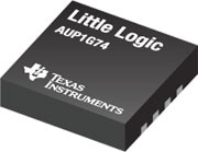
SN74AUP1G74
Low-Power Single Positive-Edge-Triggered D-Type Flip-Flop
Click for more information.
- Available in the Texas Instruments NanoStar™ Package
- Low Static-Power Consumption: ICC = 0.9 µA Max
- Low Dynamic-Power Consumption: Cpd = 5.5 pF Typ at 3.3 V
- Low Input Capacitance: Ci = 1.5 pF Typ
- Low Noise – Overshoot and Undershoot <10% of VCC
- Ioff Supports Partial-Power-Down Mode Operation
- Schmitt-Trigger Action Allows Slow Input Transition and Better Switching Noise Immunity at the Input (Vhys = 250 mV Typ at 3.3 V)
- Wide Operating VCC Range of 0.8 V to 3.6 V
- Optimized for 3.3-V Operation
- 3.6-V I/O Tolerant to Support Mixed-Mode Signal Operation
- tpd = 5 ns Max at 3.3 V
- Suitable for Point-to-Point Applications
- Latch-Up Performance Exceeds 100 mA Per JESD 78, Class II
- ESD Performance Tested Per JESD 22
- 2000-V Human-Body Model (A114-B, Class II)
- 1000-V Charged-Device Model (C101)


SN74AUP1G79
Low-Power Single Positive-Edge-Triggered D-Type Flip-Flop
Click for more information.
- Available in the Texas Instruments NanoStar™ Package
- Low Static-Power Consumption:
ICC = 0.9 µA Max
- Low Dynamic-Power Consumption:
Cpd = 3 pF Typ at 3.3 V
- Low Input Capacitance:
Ci = 1.5 pF Typ
- Low Noise: Overshoot and Undershoot
<10% of VCC
- Ioff Supports Partial Power-Down-Mode Operation
- Input Hysteresis Allows Slow Input Transition and Better Switching
Noise Immunity at the Input (Vhys = 250 mV Typ at 3.3 V)
- Wide Operating VCC Range of 0.8 V to 3.6 V
- Optimized for 3.3-V Operation
- 3.6-V I/O Tolerant to Support Mixed-Mode Signal Operation
- tpd = 4 ns Max at 3.3 V
- Suitable for Point-to-Point Applications
- Latch-Up Performance Exceeds 100 mA Per JESD 78, Class II
- ESD Performance Tested Per JESD 22
- 2000-V Human-Body Model
(A114-B, Class II)
- 1000-V Charged-Device Model (C101)


SN74LVC1G04
Single Inverter
Click for more information.
- Available in the Texas Instruments NanoFree™ Package
- Supports 5-V VCC Operation
- Inputs Accept Voltages to 5.5 V
- Max tpd of 3.3 ns at 3.3 V
- Low Power Consumption, 10-µA Max ICC
- ±24-mA Output Drive at 3.3 V
- Ioff Supports Live Insertion, Partial Power
Down Mode, and Back Drive Protection
- Latch-Up Performance Exceeds 100 mA Per JESD 78, Class II
- ESD Protection Exceeds JESD 22
- 2000-V Human-Body Model (A114-A)
- 200-V Machine Model (A115-A)
- 1000-V Charged-Device Model (C101)


SN74LVC1G07
Single Buffer/Driver With Open-Drain Output
Click for more information.
- Available in the Texas Instruments
NanoFree Package
- Supports 5-V VCC Operation
- Input and Open-Drain Output Accept
Voltages up to 5.5 V
- Max tpd of 4.2 ns at 3.3 V
- Low Power Consumption, 10-µA Max ICC
- ±24-mA Output Drive at 3.3 V
- Ioff Supports Partial-Power-Down Mode
Operation
- Latch-Up Performance Exceeds 100 mA Per
JESD 78, Class II
- ESD Protection Exceeds JESD 22
- 2000-V Human-Body Model (A114-A)
- 200-V Machine Model (A115-A)
- 1000-V Charged-Device Model (C101)


SN74LVC1G08
Single 2-Input Positive-AND Gate
Click for more information.
- Available in the Texas Instruments NanoFree™ Package
- Supports 5-V VCC Operation
- Inputs Accept Voltages to 5.5 V
- Max tpd of 3.6 ns at 3.3 V
- Low Power Consumption, 10-µA Max ICC
- ±24-mA Output Drive at 3.3 V
- Ioff Supports Partial-Power-Down Mode Operation
- Latch-Up Performance Exceeds 100 mA Per JESD 78, Class II
- ESD Protection Exceeds JESD 22
- 2000-V Human-Body Model (A114-A)
- 200-V Machine Model (A115-A)
- 1000-V Charged-Device Model (C101)

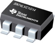
SN74LVC1G14
Single Schmitt-Trigger Inverter
Click for more information.
- Available in the Texas Instruments NanoStar and NanoFree Packages
- Supports 5-V VCC Operation
- Inputs Accept Voltages to 5.5 V
- Max tpd of 4.6 ns at 3.3 V
- Low Power Consumption, 10-µA Max ICC
- ±24-mA Output Drive at 3.3 V
- Ioff Supports Live Insertion, Partial Power Down Mode, and Back Drive Protection
- Latch-Up Performance Exceeds 100 mA Per JESD 78, Class II
- ESD Protection Exceeds JESD 22
- 2000-V Human-Body Model (A114-A)
- 200-V Machine Model (A115-A)
- 1000-V Charged-Device Model (C101)


SN74LVC1G17
Single Schmitt-Trigger Buffer
Click for more information.
- Available in the Texas Instruments NanoFree Package
- Supports 5-V VCC Operation
- Inputs Accept Voltages to 5.5 V
- Max tpd of 4.6 ns at 3.3 V
- Low Power Consumption, 10-µA Max ICC
- ±24-mA Output Drive at 3.3 V
- Ioff Supports Live Insertion, Partial Power Down Mode, and Back Drive Protection
- Latch-Up Performance Exceeds 100 mA Per JESD 78, Class II
- ESD Protection Exceeds JESD 22
- 2000-V Human-Body Model (A114-A)
- 200-V Machine Model (A115-A)
- 1000-V Charged-Device Model (C101)


SN74LVC1G32
Single 2-Input Positive-OR Gate
Click for more information.
- Available in the Texas Instruments NanoStar™ and NanoFree™ Packages
- Supports 5-V VCC Operation
- Inputs Accept Voltages to 5.5 V
- Max tpd of 3.6 ns at 3.3 V
- Low Power Consumption, 10-µA Max IC C
- ±24-mA Output Drive at 3.3 V
- Ioff Supports Partial-Power-Down Mode Operation
- Latch-Up Performance Exceeds 100 mA Per JESD 78, Class II
- ESD Protection Exceeds JESD 22
- 2000-V Human-Body Model (A114-A)
- 200-V Machine Model (A115-A)
- 1000-V Charged-Device Model (C101)


SN74LVC1G123
Single Retriggerable Monostable Multivibrator with Schmitt-Trigger Inputs
Click for more information.
- Available in the Texas Instruments NanoFree™ Package
- Supports 5-V VCC Operation
- Inputs Accept Voltages to 5.5 V
- Max tpd of 8 ns at 3.3 V
- Supports Mixed-Mode Voltage Operation on All Ports
- Schmitt-Trigger Circuitry on A and B Inputs for Slow Input Transition Rates
- Edge Triggered From Active-High or Active-Low Gated Logic Inputs
- Retriggerable for Very Long Output Pulses, up to 100% Duty Cycle
- Overriding Clear Terminates Output Pulse
- Glitch-Free Power-Up Reset on Outputs
- Ioff Supports Partial-Power-Down Mode Operation
- Latch-Up Performance Exceeds 100 mA Per JESD 78, Class II
- ESD Protection Exceeds JESD 22
- 2000-V Human-Body Model (A114-A)
- 200-V Machine Model (A115-A)
- 1000-V Charged-Device Model (C101)


SN74LVC1G125
Single Bus Buffer Gate With 3-State Outputs
Click for more information.
- Available in the Texas Instruments NanoFree™ Package
- Supports 5-V VCC Operation
- Inputs Accept Voltages to 5.5 V
- Max tpd of 3.7 ns at 3.3 V
- Low Power Consumption, 10-µ A Max ICC
- ±24-mA Output Drive at 3.3 V
- Ioff Supports Partial-Power-Down Mode Operation
- Latch-Up Performance Exceeds 100 mA Per JESD 78, Class II
- ESD Protection Exceeds JESD 22
- 2000-V Human-Body Model (A114-A)
- 200-V Machine Model (A115-A)
- 1000-V Charged-Device Model (C101)


SN74LVC1G332
Single 3-Input Positive-OR Gate
Click for more information.
- Available in the Texas Instruments NanoStar™ and NanoFree™ Packages
- Supports 5-V VCC Operation
- Inputs Accept Voltages to 5.5 V
- Max tpd of 4.5 ns at 3.3 V
- Low Power Consumption, 10-µA Max ICC
- ±24-mA Output Drive at 3.3 V
- Ioff Supports Partial-Power-Down Mode Operation
- Latch-Up Performance Exceeds 100 mA Per
JESD 78, Class II
- ESD Protection Exceeds JESD 22
- 2000-V Human-Body Model (A114-A)
- 200-V Machine Model (A115-A)
- 1000-V Charged-Device Model (C101)

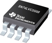
SN74LVC2G08
Dual 2-Input Positive-AND Gate
Click for more information.
- Available in the Texas Instruments NanoFree™ Package
- Supports 5-V VCC Operation
- Inputs Accept Voltages to 5.5 V
- Max tpd of 4.7 ns at 3.3 V
- Low Power Consumption, 10-µA Max ICC
- ±24-mA Output Drive at 3.3 V
- Typical VOLP (Output Ground Bounce) <0.8 V at VCC = 3.3 V, TA = 25°C
- Typical VOHV (Output VOH Undershoot)>2 V at VCC = 3.3 V, TA = 25°C
- Ioff Supports Partial-Power-Down Mode Operation
- Latch-Up Performance Exceeds 100 mA Per JESD 78, Class II
- ESD Protection Exceeds JESD 22
- 2000-V Human-Body Model (A114-A)
- 1000-V Charged-Device Model (C101)

Logic
As the world leader in logic, Texas Instruments (TI) offers a full spectrum of logic functions and technologies ranging from the mature bipolar and bipolar complementary metal-oxide semiconductor (BiCMOS) families to the latest advanced CMOS families. TI offers process technologies with the logic performance and features needed in today’s electronic markets while maintaining support for traditional logic products. TI’s product offerings include the following process technologies or device families:
- AC, ACT, AHC, AHCT, ALVC, AUC, AUP, AVC, FCT, HC, HCT, LV-A, LV-AT, LVC, TVC
- ABT, ABTE, ALB, ALVT, BCT, HSTL, LVT
- BTA, CB3Q, CB3T, CBT, CBT-C, CBTLV, FB, FIFOs, GTL, GTLP, JTAG, I2C, VME
- ALS, AS, F, LS, S, TTL
SN74LVC00ARGYR
Quadruple 2-Input Positive-NAND Gate
Click for more information.
- Operate From 1.65 V to 3.6 V
- Specified From -40°C to 85°C, -40°C to 125°C, and -55°C to 125°C
- Inputs Accept Voltages to 5.5 V
- Max tpd of 4.3 ns at 3.3 V
- Typical VOLP (Output Ground Bounce) <0.8 V at VCC = 3.3 V, TA = 25°C
- Typical VOHV (Output VOH Undershoot) >2 V at VCC = 3.3 V, TA = 25°C
- Latch-Up Performance Exceeds 250 mA Per JESD 17
- ESD Protection Exceeds JESD 22
- 2000-V Human-Body Model (A114-A)
- 200-V Machine Model (A115-A)
- 1000-V Charged-Device Model (C101)

SN74LVC06ARGYR
Hex Inverter Buffers/Drivers With Open-Drain Outputs
Click for more information.
- Operate From 1.65 V to 3.6 V
- Specified From -40°C to 85°C, -40°C to 125°C, and -55°C to 125°C
- Inputs and Open-Drain Outputs Accept Voltages up to 5.5 V
- Max tpd of 3.7 ns at 3.3 V
- Ioff Supports Partial-Power-Down Mode Operation
- Latch-Up Performance Exceeds 250 mA Per JESD 17

SN74LVC08ARGYR
Quadruple 2-Input Positive-AND Gate
Click for more information.
- Operate From 1.65 V to 3.6 V
- Specified From –40°C to 85°C, –40°C to 125°C, and –55°C to 125°C
- Inputs Accept Voltages to 5.5 V
- Max tpd of 4.1 ns at 3.3 V
- Typical VOLP (Output Ground Bounce) <0.8 V at VCC = 3.3 V, TA = 25°C
- Typical VOHV (Output VOH Undershoot) >2 V at VCC = 3.3 V, TA = 25°C
- Latch-Up Performance Exceeds 250 mA Per JESD 17
- ESD Protection Exceeds JESD 22
- 2000-V Human-Body Model (A114-A)
- 200-V Machine Model (A115-A)
- 1000-V Charged-Device Model (C101)

TS3L110
Quad SPDT High-Bandwidth 10/100 Base-T Lan Switch Differential 8 to 4 Multiplexer/Demultiplexer
Click for more information.
- Wide Bandwidth (BW = 500 MHz Typ)
- Low Crosstalk (XTALK = –30 dB Typ)
- Bidirectional Data Flow, With Near-Zero Propagation Delay
- Low and Flat ON-State Resistance (ron = 4 Ω)
- Switching on Data I/O Ports (0 to 5 V)
- VCC Operating Range From 3 V to 3.6 V
- Ioff Supports Partial-Power-Down Mode Operation
- Data and Control Inputs Have Undershoot Clamp Diodes
- Latch-Up Performance Exceeds 100 mA Per JESD 78, Class II
- ESD Performance Tested Per JESD 22
- 2000-V Human-Body Model (A114-B, Class II)
- 1000-V Charged-Device Model (C101)
- Suitable for Both 10 Base-T/100 Base-T Signaling


CD4011B
CMOS Quad 2-Input NAND Gate
Click for more information.
- Propagation delay time = 60 ns (typ.) at CL = 50 pF, VDD = 10 V
- Buffered inputs and outputs
- Standardized symmetrical output characteristics
- Maximum input current of 1 µA at 18 V over-full package temperature range; 100 nA at 18 V and 25°C
- 100% tested for quiescent current at 20 V
- 5-V, 10-V, and 15-V parametric ratings
- Noise margin (over full package temperature range:
1 V at VDD = 5 V
2 V at VDD = 10 V
2.5 at VDD = 15 V
- Meets all requirements of JEDEC Tentative Standard No. 13B, "Standard Specifications for Description of "B" Series CMOS Devices"

CD4013B
CMOS Dual D-Type Flip Flop
Click for more information.
- Set-Reset capability
- Static flip-flop operation — retains state indefinitely with clock level either "high" or "low"
- Medium-speed operation — 16MHz (typ.) clock toggle rate at 10 V
- Standardized, symmetrical output characteristics
- 100% tested for quiescent current at 20 V
- Maximum input current of 1 µA at 18 V over full package-temperature range; 100 nA at 18 V and 25°C
- Noise margin (full package-temperature range) =
- 1 V at VDD = 5 V
- 2 V at VDD = 10 V
- 2.5 V at VDD = 15 V
- 5-V, 10-V, and 15-V parametric ratings
- Meets all requirements of JEDEC Tentative Standard No. 13B, "Standard Specifications for Description of ’B’ Series CMOS Devices"
- Applications:
- Registers, counters, control circuits

CD4017B
CMOS Decade Counter with 10 Decoded Outputs
Click for more information.
- Fully static operation
- Medium speed operation…10 MHz (typ.) at VDD = 10 V
- Standardized, symmetrical output characteristics
- 100% tested for quiescent current at 20 V
- 5-V, 10-V, and 15-V parametric ratings
- Meets all requirements of JEDEC Tentative Standard No. 13B, "Standard Specifications for Description of ’B’ Series CMOS Devices"
- Applications:
- Decade counter/decimal decode display (CD4017B)
- Binary counter/decoder
- Frequency division
- Counter control/timers
- Divde-by-N counting
- For further application information, see ICAN-6166 "COS/MOS MSI Counter and Register Design and Applications"

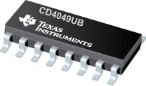
CD4049UB
CMOS Hex Inverting Buffer/Converter
Click for more information.
- CD4049UB Inverting
- CD4050B Non-Inverting
- High Sink Current for Driving 2 TTL Loads
- High-To-Low Level Logic Conversion
- 100% Tested for Quiescent Current at 20V
- Maximum Input Current of 1µA at 18V Over Full Package Temperature Range; 100nA at 18V and 25°C
- 5V, 10V and 15V Parametric Ratings
- Applications
- CMOS to DTL/TTL Hex Converter
- CMOS Current "Sink" or "Source" Driver
- CMOS High-To-Low Logic Level Converter

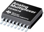
CD4051B
CMOS Single 8-Channel Analog Multiplexer/Demultiplexer with Logic-Level Conversion
Click for more information.
- Wide Range of Digital and Analog Signal Levels
- Digital...3V to 20V
- Analog...≤20VP-P
- Low ON Resistance, 125Ω(Typ) Over 15VP-P Signal Input Range for VDD–VEE = 18V
- High OFF Resistance, Channel Leakage of ±100pA (Typ) at VDD–VEE = 18V
- Logic-Level Conversion for Digital Addressing Signals of 3V to 20V (VDD–VSS = 3V to 20V) to Switch Analog Signals to 20VP-P (VDD–VEE = 20V)
- Matched Switch Characteristics, rON = 5Ω (Typ) for VDD–VEE = 15V
- Very Low Quiescent Power Dissipation Under All Digital-Control Input and Supply Conditions, 0.2µW (Typ) at VDD–VSS = VDD–VEE = 10V
- Binary Address Decoding on Chip
- 5V, 10V and 15V Parametric Ratings
- 10% Tested for Quiescent Current at 20V
- Maximum Input Current of 1µA at 18V Over Full Package Temperature Range, 100nA at 18V and 25°C
- Break-Before-Make Switching Eliminates Channel Overlap
- Applications
- Analog and Digital Multiplexing and Demultiplexing
- A/D and D/A Conversion
- Signal Gating

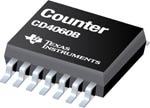
CD4060B
CMOS 14-Stage Ripple-Carry Binary Counter/Divider and Oscillator
Click for more information.
- 12 MHz clock rate at 15 V
- Common reset
- Fully static operation
- Buffered inputs and outputs
- Schmitt trigger input-pulse line
- 100% tested for quiescent current at 20 V
- Standardized, symmetrical output characteristics
- 5-V, 10-V, and 15-V parametric ratings
- Meets all requirements of JEDEC Tentative Standard No. 13B, "Standard Specifications for Description of ’B’ Series CMOS Devices’
- Oscillator Features:
- All active components on chip
- RC or crystal oscillator configuration
- RC oscillator frequency of 690 kHz min. at 15 V
- Applications
- Control counters
- Timers
- Frequency dividers
- Time-delay circuits

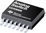
CD4066B
CMOS Quad Bilateral Switch
Click for more information.
- 15-V Digital or ±7.5-V Peak-to-Peak Switching
- 125-Ω Typical On-State Resistance for 15-V Operation
- Switch On-State Resistance Matched to Within 5 Ω Over 15-V Signal-Input Range
- On-State Resistance Flat Over Full Peak-to-Peak Signal Range
- High On/Off Output-Voltage Ratio: 80 dB Typical at fis = 10 kHz, RL = 1 kΩ
- High Degree of Linearity: <0.5% Distortion Typical at fis = 1 kHz, Vis = 5 V p-p, VDD–VSS Ω
- Extremely Low Off-State Switch Leakage, Resulting in Very Low Offset Current and High Effective Off-State Resistance: 10 pA Typical at VDD–VSS = 10 V, TA = 25°C
- Extremely High Control Input Impedance (Control Circuit Isolated From Signal Circuit): 1012 Ω Typical
- Low Crosstalk Between Switches: –50 dB Typical at fis = 8 MHz, RL = 1 kΩ
- Matched Control-Input to Signal-Output Capacitance: Reduces Output Signal Transients
- Frequency Response, Switch on = 40 MHz (Typical)
- 100% Tested for Quiescent Current at 20 V
- 5-V, 10-V, and 15-V Parametric Ratings
- Meets All Requirements of JEDEC Tentative Standard No. 13B, Standard Specifications for Description of B-Series CMOS Devices
- Applications:
- Analog Signal Switching/Multiplexing:
Signal Gating, Modulator, Squelch Control, Demodulator, Chopper, Commutating Switch
- Digital Signal Switching/Multiplexing
- Transmission-Gate Logic Implementation
- Analog-to-Digital and Digital-to-Analog Conversion
- Digital Control of Frequency, Impedance, Phase, and Analog-Signal Gain

CD4093B
CMOS Quad 2-Input NAND Schmitt Triggers
Click for more information.
- Schmitt-trigger action on each input with no external components
- Hysteresis voltage typically 0.9 V at VDD = 5 V and 2.3 V at VDD = 10 V
- Noise immunity greater than 50%
- No limit on input rise and fall times
- Standardized, symmetrical output characteristics
- 100% tested for quiescent current at 20 V
- Maximum input current of 1 µA at 18 V over full package-temperature range, 100 nA at 18 V and 25°C
- 5-V, 10-V, and 15-V parametric ratings
- Meets all requirements of JEDEC Tentative Standard No. 13B, "Standard Specifications for Description of 'B' Series CMOS Devices"
- Applications:
- Wave and pulse shapers
- High-noise-environment systems
- Monostable multivibrators
- Astable multivibrators
- NAND logic


CD74HC154
High Speed CMOS Logic 4-to-16 Line Decoder/Demultiplexer
Click for more information.
- Two Enable Inputs to Facilitate Demultiplexing and Cascading Functions
- Fanout (Over Temperature Range)
- Standard Outputs . . . . . . 10 LSTTL Loads
- Bus Driver Outputs . . . 15 LSTTL Loads
- Wide Operating Temperature Range . . . –55°C to 125°C
- Balanced Propagation Delay and Transition Times
- Significant Power Reduction Compared to LSTTL Logic ICs
- HC Types
- 2V to 6V Operation
- High Noise Immunity: NIL= 30%, NIH = 30% of VCC at VCC = 5V
- HCT Types
- 4.5V to 5.5V Operation
- Direct LSTTL Input Logic Compatibility, VIL = 0.8V (Max), VIH = 2V (Min)
- CMOS Input Compatibility, Il
 1µA at VOL, VOH 1µA at VOL, VOH

SN7400
Quad 2-input positive-NAND gates
Click for more information.
- Package Options Include Plastic Small-Outline (D, NS, PS), Shrink Small-Outline (DB), and Ceramic Flat (W) Packages, Ceramic Chip Carriers (FK), and Standard Plastic (N) and Ceramic (J) DIPs
- Also Available as Dual 2-Input Positive-NAND Gate in Small-Outline (PS) Package


SN7404
Hex inverters
Click for more information.
- Dependable Texas Instruments Quality and Reliability

SN74HC14
Hex Schmitt-Trigger Inverters
Click for more information.
- Wide Operating Voltage Range of 2 V to 6 V
- Outputs Can Drive Up To 10 LSTTL Loads
- Low Power Consumption, 20-µA Max ICC
- Typical tpd = 11 ns
- ±4-mA Output Drive at 5 V
- Low Input Current of 1 µA Max

SN74LS00
Quad 2-input positive-NAND gates
Click for more information.
- Package Options Include Plastic Small-Outline (D, NS, PS), Shrink Small-Outline (DB), and Ceramic Flat (W) Packages, Ceramic Chip Carriers (FK), and Standard Plastic (N) and Ceramic (J) DIPs
- Also Available as Dual 2-Input Positive-NAND Gate in Small-Outline (PS) Package


SN74LS04
Hex inverters
Click for more information.
- Dependable Texas Instruments Quality and Reliability

SN74LS08
Quadruple 2-Input Positive-AND Gates
Click for more information.
- Package Options Include Plastic “Small Outline" Packages, Ceramic Chip Carriers and Flat Packages, and Plastic and Ceramic DIPs
- Dependable Texas Instruments Quality and Reliability


SN74CB3Q16211
24-Bit FET 2.5-V/3.3-V Low-Voltage High-Bandwidth Bus Switch
Click for more information.
- Member of the Texas Instruments Widebus™ Family
- High-Bandwidth Data Path (Up To 500 MHz
 ) )
- 5-V Tolerant I/Os with Device Powered Up or Powered Down
- Low and Flat ON-State Resistance (ron) Characteristics Over Operating Range (ron = 5 Ω Typical)
- Rail-to-Rail Switching on Data I/O Ports
- 0-V to 5-V Switching With 3.3-V VCC
- 0-V to 3.3-V Switching With 2.5-V VCC
- Bidirectional Data Flow, With Near-Zero Propagation Delay
- Low Input/Output Capacitance Minimizes Loading and Signal Distortion (Cio(OFF) = 4 pF Typical)
- Fast Switching Frequency (fOE\ = 20 MHz Max)
- Data and Control Inputs Provide Undershoot Clamp Diodes
- Low Power Consumption (ICC = 1 mA Typical)
- VCC Operating Range From 2.3 V to 3.6 V
- Data I/Os Support 0-V to 5-V Signaling Levels (0.8 V, 1.2 V, 1.5 V, 1.8 V, 2.5 V, 3.3 V, 5 V)
- Control Inputs Can be Driven by TTL or 5-V/3.3-V CMOS Outputs
- Ioff Supports Partial-Power-Down Mode Operation
- Latch-Up Performance Exceeds 100 mA Per JESD 78, Class II
- ESD Performance Tested Per JESD 22
- 2000-V Human-Body Model (A114-B, Class II)
- 1000-V Charged-Device Model (C101)

SN74LVC138A
3-Line To 8-Line decoder/Demultiplexer
Click for more information.
- Operate From 1.65 V to 3.6 V
- Inputs Accept Voltages to 5.5 V
- Max tpd of 5.8 ns at 3.3 V
- Typical VOLP (Output Ground Bounce)
< 0.8 V at VCC = 3.3 V, TA = 25°C
- Typical VOHV (Output VOH Undershoot)
> 2 V at VCC = 3.3 V, TA = 25°C
- Latch-Up Performance Exceeds 250 mA Per JESD 17
- ESD Protection Exceeds JESD 22
- 2000-V Human-Body Model (A114-A)
- 200-V Machine Model (A115-A)
- 1000-V Charged-Device Model (C101)

Standard Linear
TI’s products dedicated to the analog market are multimarket, general purpose products including signal conditioning circuits, power management, interface products and data converters. TI has developed the industry’s largest selection of low-power and low-voltage analog parts with features designed to satisfy an extensive range of applications. TI Standard Linear products offer:
- Small packaging
- High Performance
- Extensive Capacity
- Application Support
LMV339
Quad General Purpose Low-Voltage Comparators
Click for more information.
- 2.7-V and 5-V Performance
- Low Supply Current
- LMV331 . . . 130 µA Typ
- LMV393 . . . 210 µA Typ
- LMV339 . . . 410 µA Typ
- Input Common-Mode Voltage Range Includes Ground
- Low Output Saturation Voltage 200 mV Typical
- Open-Collector Output for Maximum Flexibility

LMV393
Dual General Purpose Low-Voltage Comparator
Click for more information.
- 2.7-V and 5-V Performance
- Low Supply Current
- LMV331 . . . 130 µA Typ
- LMV393 . . . 210 µA Typ
- LMV339 . . . 410 µA Typ
- Input Common-Mode Voltage Range Includes Ground
- Low Output Saturation Voltage 200 mV Typical
- Open-Collector Output for Maximum Flexibility

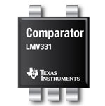
LMV331
Single General Purpose Low-Voltage Comparator
Click for more information.
- 2.7-V and 5-V Performance
- Low Supply Current
- LMV331 . . . 130 µA Typ
- LMV393 . . . 210 µA Typ
- LMV339 . . . 410 µA Typ
- Input Common-Mode Voltage Range Includes Ground
- Low Output Saturation Voltage 200 mV Typical
- Open-Collector Output for Maximum Flexibility


LM311
Differential Comparator With Strobes
Click for more information.
- Fast Response Times
- Strobe Capability
- Maximum Input Bias Current . . . 300 nA
- Maximum Input Offset Current . . . 70 nA
- Can Operate From Single 5-V Supply
- Available in Q-Temp Automotive
- High-Reliability Automotive Applications
- Configuration Control/Print Support
- Qualification to Automotive Standards

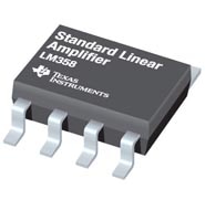
LM358
Dual Operational Amplifiers
Click for more information.
- Wide Supply Range:
- Single Supply . . . 3 V to 32 V
(26 V for LM2904)
- or Dual Supplies . . . ±1.5 V to ±n;16 V
(±13 V for LM2904)
- Low Supply-Current Drain Independent of Supply Voltage . . . 0.7 mA Typ
- Common-Mode Input Voltage Range Includes Ground, Allowing Direct Sensing Near Ground
- Low Input Bias and Offset Parameters:
- Input Offset Voltage ...3 mV Typ
A Versions ...2 mV Typ
- Input Offset Current ...2 nA Typ
- Input Bias Current . . . 20 nA Typ
A Versions . . . 15 nA Typ
- Differential Input Voltage Range Equal to Maximum-Rated Supply Voltage . . . ±32 V
(26 V for LM2904)
- Open-Loop Differential Voltage Amplification . . . 100 V/mV Typ
- Internal Frequency Compensation

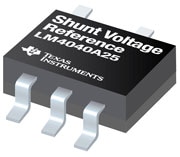
LM4040A25
2.5-V Precision Micropower Shunt Voltage Reference, 0.1% accuracy
Click for more information.
- Fixed Output Voltages of 2.048 V, 2.5 V, 3 V, 4.096 V, 5 V, 8.192 V, and 10 V
- Tight Output Tolerances and LowTemperature Coefficient
- Max 0.1%, 100 ppm/°C - A Grade
- Max 0.2%, 100 ppm/°C - B Grade
- Max 0.5%, 100 ppm/°C - C Grade
- Max 1.0%, 150 ppm/°C - D Grade
- Low Output Noise. . .35 µVRMS Typ
- Wide Operating Current Range. . .45 µA Typ to 15 mA
- Stable With All Capacitive Loads; No Output Capacitor Required
- Available in Extended Temperature Range. . .-40°C to 125°C
- APPLICATIONS
- Data-Acquisition Systems
- Power Supplies and Power-Supply Monitors
- Instrumentation and Test Equipment
- Process Controls
- Precision Audio
- Automotive Electronics
- Energy Management
- Battery-Powered Equipment

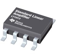
LT1013
Dual Precision Operational Amplifier
Click for more information.
- Single-Supply Operation
- Input Voltage Range Extends to Ground
- Output Swings to Ground While Sinking Current
- Input Offset Voltage
- 150 µV Max at 25°C for LT1013A
- Offset-Voltage Temperature Coefficient
- 2.5 µV/°C Max for LT1013A
- Input Offset Current
- 0.8 nA Max at 25°C for LT1013A
- High Gain . . . 1.5 V/µV Min (RL = 2 kΩ), 0.8 V/µV Min (RL = 600 kΩ) for LT1013A
- Low Supply Current . . . 0.5 mA Max at TA = 25°C for LT1013A
- Low Peak-to-Peak Noise Voltage . . . 0.55 µV Typ
- Low Current Noise . . . 0.07 pA/√Hz Typ

NE5532
Dual Low-Noise High-Speed Audio Operational Amplifier
Click for more information.
- Equivalent Input Noise Voltage:
5 nV/√Hz Typ at 1 kHz
- Unity-Gain Bandwidth: 10 MHz Typ
- Common-Mode Rejection Ratio: 100 dB Typ
- High DC Voltage Gain: 100 V/mV Typ
- Peak-to-Peak Output Voltage Swing 26 V Typ
With VCC± = ±15 V and RL = 600 Ω
- High Slew Rate: 9 V/µs Typ

RC4558
Dual General-Purpose Operational Amplifier
Click for more information.
- Continuous Short-Circuit Protection
- Wide Common-Mode and Differential Voltage Ranges
- No Frequency Compensation Required
- Low Power Consumption
- No Latch-Up
- Unity-Gain Bandwidth . . . 3 MHz Typ
- Gain and Phase Match Between Amplifiers
- Low Noise . . . 8 nV/√Hz Typ at 1 kHz

TL431
Adjustable Precision Shunt Regulator
Click for more information.
- Operation From −40°C to 125°C
- Reference Voltage Tolerance at 25°C
- 0.5% . . . B Grade
- 1%. . . A Grade
- 2% . . . Standard Grade
- Typical Temperature Drift (TL431B)
- 6 mV (C Temp)
- 14 mV (I Temp, Q Temp)
- Low Output Noise
- 0.2-Ω Typical Output Impedance
- Sink-Current Capability . . . 1 mA to 100 mA
- Adjustable Output Voltage . . . Vref to 36 V

TL072
Dual Low-Noise JFET-Input General-Purpose Operational Amplifier
Click for more information.
- Low Power Consumption
- Wide Common-Mode and Differential Voltage Ranges
- Low Input Bias and Offset Currents
- Output Short-Circuit Protection
- Low Total Harmonic Distortion ... 0.003% Typ
- Low Noise
Vn = 18 nV/√Hz Typ at f = 1 kHz
- High Input Impedance . . . JFET Input Stage
- Internal Frequency Compensation
- Latch-Up-Free Operation
- High Slew Rate . . . 13 V/µs Typ
- Common-Mode Input Voltage Range Includes VCC+

TL074
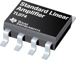
Quad Low-Noise JFET-Input General-Purpose Operational Amplifier
Click for more information.
- Low Power Consumption
- Wide Common-Mode and Differential Voltage Ranges
- Low Input Bias and Offset Currents
- Output Short-Circuit Protection
- Low Total Harmonic Distortion ... 0.003% Typ
- Low Noise
Vn = 18 nV/√Hz Typ at f = 1 kHz
- High Input Impedance . . . JFET Input Stage
- Internal Frequency Compensation
- Latch-Up-Free Operation
- High Slew Rate . . . 13 V/µs Typ
- Common-Mode Input Voltage Range Includes VCC+

TL084
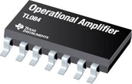
JFET-Input Operational Amplifier
Click for more information.
- Low Power Consumption
- Wide Common-Mode and Differential Voltage Ranges
- Low Input Bias and Offset Currents
- Output Short-Circuit Protection
- Low Total Harmonic Distortion...0.003% Typ
- High Input Impedance...JFET-Input Stage
- Latch-Up-Free Operation
- High Slew Rate...13 V/µs Typ
- Common-Mode Input Voltage Range Includes VCC+

UA741
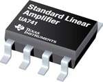
General-Purpose Operational Amplifier
Click for more information.
- Short-Circuit Protection
- Offset-Voltage Null Capability
- Large Common-Mode and Differential Voltage Ranges
- No Frequency Compensation Required
- Low Power Consumption
- No Latch-Up
- Designed to Be Interchangeable With Fairchild uA741


L293D
Quadruple Half-H Drivers
Click for more information.
- Featuring Unitrode L293 and L293D Products Now From Texas Instruments
- Wide Supply-Voltage Range: 4.5 V to 36 V
- Separate Input-Logic Supply
- Internal ESD Protection
- Thermal Shutdown
- High-Noise-Immunity Inputs
- Functional Replacements for SGS L293 and SGS L293D
- Output Current 1 A Per Channel (600 mA for L293D)
- Peak Output Current 2 A Per Channel (1.2 A for L293D)
- Output Clamp Diodes for Inductive Transient Suppression (L293D)

LMV321
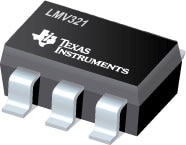
Single Low-Voltage Rail-to-Rail Output Operational Amplifier
Click for more information.
- 2.7-V and 5-V Performance
- -40°C to 125°C Operation
- Low-Power Shutdown Mode (LMV324S)
- No Crossover Distortion
- Low Supply Current
- LMV321 . . . 130 µA Typ
- LMV358 . . . 210 µA Typ
- LMV324 . . . 410 µA Typ
- LMV324S . . . 410 µA Typ
- Rail-to-Rail Output Swing
- ESD Protection Exceeds JESD 22
- 2000-V Human-Body Model (A114-A)
- 1000-V Charged-Device Model (C101)


MAX232
Dual EIA-232 Driver/Receiver
Click for more information.
- Meet or Exceed TIA/EIA-232-F and ITU Recommended V.28
- Operates From a Single 5-V Power Supply With 1.0-µF Charge-Pump Capacitors
- Operate Up To 120 kbit/s
- Two Drivers and Two Receivers
- ±30-V Input Levels
- Low Supply Current ...8 mA Typical
- ESD Protection Exceeds JESD 22
- 2000-V Human-Body Model (A114-A)
- Upgrade With Improved ESD (15-kV HBM) and 0.1-µF Charge-Pump Capacitors is Available With the MAX202
- Applications
- TIA/EIA-232-F, Battery-Powered Systems, Terminals, Modems, and Computers


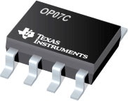
OP07C
Low-Offset Voltage Operational Amplifier
Click for more information.
- Low Noise
- No External Components Required
- Replace Chopper Amplifiers at a Lower Cost
- Wide Input-Voltage Range
. . . 0 to ±14 V Typ
- Wide Supply-Voltage Range
. . . ±3 V to ±18 V

ESD/EMI
System-level electrostatic discharge (ESD) protection has become very important in today’s world as devices become portable, contain multiple interface connectors, have touchscreens and are continually exposed to the external world. It only takes one ESD strike to permanently damage a product, making ESD protection a critical component of system design. Electromagnetic interference (EMI) is another challenge often faced in system design. EMI is a radio frequency (RF) (800 MHz to 2 GHz) disturbance that affects an electrical circuit due to electromagnetic conduction from an external source. Texas Instruments produces both ESD and EMI devices with solutions that protect the majority of external connections to the outside world.
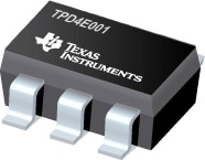
TPD4E001
Low-Capacitance 4-Channel +/-15-kV ESD Protection Array
Click for more information.
- 4-Channel ESD Clamp Array to Enhance System-Level ESD Protection
- Exceeds IEC61000-4-2 (Level 4) ESD Protection Requirement
- ±8-kV IEC 61000-4-2 Contact Discharge
- ±15-kV IEC 61000-4-2 Air-Gap Discharge
- ±15-kV Human-Body Model (HBM)
- 5.5-A Peak Pulse Current (8/20-us Pulse)
- Low 1.5-pF Input Capacitance

TPD4S014
A Complete Single-chip Solution for USB Charger Port Protection
Click for more information.
- Input Voltage Protection at VBUS up to 28V
- Low Ron nFET Switch
- Supports >2A charging current
- Over Voltage and Under Voltage Lock Out Features


TPD4E001
Low-Capacitance 4-Channel +/-15-kV ESD Protection Array for High-Speed Data Interfaces
Click for more information.
- 4-Channel ESD Clamp Array to Enhance System-Level ESD Protection
- Exceeds IEC61000-4-2 (Level 4) ESD Protection Requirements
- ±8-kV IEC 61000-4-2 Contact Discharge
- ±15-kV IEC 61000-4-2 Air-Gap Discharge
- ±15-kV Human-Body Model (HBM)
- 5.5-A Peak Pulse Current (8/20-µs Pulse)
- Low 1.5-pF Input Capacitance
- Low 1-nA (Max) Leakage Current
- 0.9-V to 5.5-V Supply-Voltage Range
- Space-Saving DRL, DBV, DCK, and DRS Package Options
- Alternate 2-, 3-, 6-Channel Options Available: TPD2E001, TPD3E001, and TPD6E001

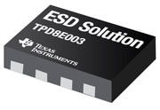
TPD8E003
8-Channel ESD Array For Portable Space-Saving Applications
Click for more information.
- 8-Channel ESD Clamp Array to Enhance System-Level ESD Protection
- Exceeds IEC61000-4-2 (Level 4) ESD Protection Requirements
- ±12-kV IEC 61000-4-2 Contact Discharge
- ±15-kV IEC 61000-4-2 Air-Gap Discharge
- 3.5-A Peak Pulse Current (8/20-µs Pulse)
- ±15-kV Human-Body Model (HBM)
- Low Breakdown Voltage of 6 V
- Low Leakage Current
- Space-Saving Ultra-Thin, Small Outline No-Lead [WSON (DQD)] Package (0.4-mm Pitch)
- APPLICATIONS
- Keypad
- Touch-Screen Interface
- Memory Interface
- Docking Connector Interface

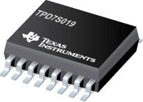
TPD7S019
7-Channel Integrated ESD Solution For VGA Port With Integrated Level Shifter
Click for more information.
- 7-Channel ESD Protection Includes ESD Protection, Level-Shifting, Buffering and Sync Impedance Matching
- Exceeds IEC61000-4-2 (Level 4) ESD Protection to Requirements on the External Pins
- ±15-kV Human-Body Model (HBM)
- ±8-kV IEC 61000-4-2 Contact Discharge
- Very Low Loading Capacitance from ESD Protection Diodes on VIDEO Lines (2.5 pF)
- 5-V Drivers for HSYNC and VSYNC Lines
- Integrated Impedance Matching Resistors on Sync Lines:
- TPD7S019-65: 65-Ω Termination
- TPD7S019-15: 15-Ω Termination
- TPD7S019-55: 55-Ω Termination
- Bi-Directional Level Shifting N-Channel FETs Provided for DDC_CLK and DDC_DATA Channels
- Flow-Through Single-In-Line Pin Mapping Ensures no Additional Board
Layout Burden while Placing the ESD Protection Chip Near the Connector
- APPLICATIONS
- VGA and DVI-I Ports in:
- Desktop and Notebook PCs
- Graphics Cards
- Set Top Boxes
- TV


TPD2S017
2-Channel Ultra Low Clamp Voltage ESD Solution with Series-Resistor Isolation
Click for more information.
- Ultra-Low Clamp Voltage Ensures the Protection of
Ultra-Low Voltage Core Chipset During ESD Events
- Exceeds ESD Protection to IEC61000-4-2 (Level 4)
- Matching of Series Resistor (R =1 Ω) of ±8 mΩ (Typical)
- Differential Channel Input Capacitance Matching of 0.02 pF (Typical)
- High-Speed Data Rate and EMI Filter Action at High Frequencies
(–3 dB Bandwidth, ≈3 GHz)
- Available in 6-Pin Small-Outline Transistor [SOT (DBV)] Package
- Flow-Through Single-In-Line Pin Mapping for the High-Speed
Lines Ensures no Additional Board Layout Burden While Placing
the ESD Protection Chip Near the Connector
- APPLICATIONS
- Hi-Speed USB
- IEEE 1394 Interface
- Low-Voltage Differential Signaling (LVDS)
- Mobile Display Digital Interface (MDDI)/Mobile
Industry Processor Interface (MIPI)
- HS Signal

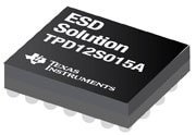
TPD12S015A
HDMI Companion Chip w/ Step-up DC-DC, I2C Level Shifter & High-speed ESD Clamps for Portable Apps
Click for more information.
- Confirms to HDMI Compliance Tests Without Any External Components
- Supports HDMI 1.4 Data Rate
- Match Class D and Class C Pin Mapping
- Excellent Matching Capacitance (0.05pF) in Each Differential Signal Pair
- Internal Boost Converter to Generate 5V From a 2.3-5.5V Battery Voltage
- Auto-direction Sensing Level Shifting in the CEC, SDA, and SCL Paths
- IEC 61000-4-2 (Level 4) System Level ESD Compliance
- Improved Drop-in Replacement for the Industry Popular TPD12S015
- Industrial Temperature Range: –40°C to 85°C

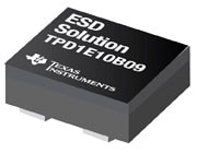
TPD1E10B09
Single Channel ESD Protection in 0402 package with 10pF Capacitance and 9V Breakdown
Click for more information.
- Provides System Level ESD Protection for Low-voltage IO Interface
- IEC 61000-4-2 Level 4
- ±20kV (Air-Gap Discharge),
- ±20kV (Contact Discharge)
- IEC 61000-4-5 (Surge): 4.5A (8/20µs)
- IO Capacitance 10pF (Typ)
- RDYN 0.5Ω (Typ)
- DC Breakdown Voltage ±9.5V (Min)
- Ultra Low Leakage Current 100nA (Typ)
- 13V Clamping Voltage (Max at IPP = 1A)
- Industrial Temperature Range: –40°C to 125°C
- Space Saving 0402 Footprint (1mm x 0.6mm x 0.5mm)

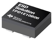
TPD1E10B06
Single Channel ESD in 0402 package with 10pF Capacitance and 6V Breakdown
Click for more information.
- Provides System Level ESD Protection for Low-voltage IO Interface
- IEC 61000-4-2 Level 4
- > ±30kV (Air-Gap Discharge),
- > ±30kV (Contact Discharge)
- IEC 61000-4-5 (Surge): 6A (8/20µs)
- IO Capacitance 12pF (Typ)
- RDYN 0.4Ω (Typ)
- DC Breakdown Voltage ±6V (Min)
- Ultra Low Leakage Current 100nA (Max)
- 10V Clamping Voltage (Max at IPP = 1A)
- Industrial Temperature Range: –40°C to 125°C
- Space Saving 0402 Footprint (1mm x 0.6mm x 0.5mm)

Analog Switches
Today’s competitive environment creates a constant need for higher performance. One common method to optimize system performance involves the use of FET switches or signal switches to provide a high-speed bidirectional bus interface between DSPs, CPUs, industry standard buses, memory and peripherals. Texas Instruments signal switch product portfolio consists of digital switches, analog switches and specialty switches that provide high-performance low-power replacements for standard bus-interface devices when signal buffering is not required.
Analog Switches

TS3DDR3812
12-Channel, 1:2 MUX/DEMUX Switch for High Speed Applications
Click for more information.
- Wide Bandwidth of 1.675 GHz
- Low Propagation Delay (tpd = 40 ps Typ)
- Low Bit-to-Bit Skew (tsk(o) = 6 ps Max)
- VCC Operating Range from 3 V to 3.6 V

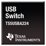
TS5USBA224
USB 2.0 High-Speed (480Mbps) and Audio Switches with Negative Signal Capability
Click for more information.
- 4 Ω High-Speed USB Switch:
- RDSON Typical
- 12.5 pF CON Typical
- 650-MHz Bandwidth (–3 dB)
- Audio Switch:
- 3 Ω RDSON Typical
- Negative Rail Capability
- Low THD: <0.05%
- Internal Shunt Resistors for Click-and-Pop Reduction
- Powered From VAUDIO (2.7V to 5.5V)
- 1.8-V Compatible Control Input (ASEL and VBUS) Threshold
- ESD Performance Tested Per JESD 22


TS5A22362
0.65-Ohm Dual SPDT Analog Switch With Negative Rail Capability
Click for more information.
- Specified Break-Before-Make Switching
- Negative Signaling Capability: Maximum Swing
From –2.75 V to 2.75 V (V+ = 2.75 V)
- Internal Shunt Switch Prevents Audible Click-and-Pop
When Switching Between Two Sources (TS5A22364)
- Low ON-State Resistance (0.65 Ω Typical)
- Low Charge Injection
- Excellent ON-State Resistance Matching
- 2.3-V to 5.5-V Power Supply (V+)
- Latch-Up Performance Exceeds 100 mA Per JESD 78, Class II
- ESD Performance Tested Per JESD 22
- 2500-V Human-Body Model (A114-B, Class II)
- 1500-V Charged-Device Model (C101)
- 200-V Machine Model (A115-A)
- APPLICATIONS
- Cell Phones
- PDAs
- Portable Instrumentation
- Audio Routing
- Medical Imaging

TS3USB221
High-Speed USB 2.0 (480 Mbps) 1:2 Multiplexer/Demultiplexer Switch With Single Enable
Click for more information.
- VCC Operation at 2.5 V and 3.3 V
- VI/O Accepts Signals up to 5.5 V
- 1.8-V Compatible Control-Pin Inputs
- Low-Power Mode When OE Is Disabled (1 µA)
- rON = 6 Ω Maximum
- ΔrON = 0.2 Ω Typical
- Cio(on) = 6 pF Maximum
- Low Power Consumption (30 µA Maximum)
- ESD > 2000-V Human-Body Model (HBM)
- High Bandwidth (1.1 GHz Typical)
- APPLICATIONS
- Routes Signals for USB 1.0, 1.1, and 2.0
- Mobile Industry Processor Interface (MIPI) Signal Routing

TS3USB30
High-Speed USB 2.0 (480 Mbps) 1:2 Multiplexer/Demultiplexer Switch With Single Enable
Click for more information.
- VCC Operation at 3 V and 4.3 V
- 1.8-V Compatible Control-Pin Inputs
- IOFF Supports Partial Power-Down-Mode Operation
- ron = 10 Ω Max
- Δron <0.35 Ω Typ
- Cio(ON) = 7 pF Typ
- Low Power Consumption (1 µA Max)
- ESD Performance Tested Per JESD 22
- 6000-V Human-Body Model (HBM)
(A114-B, Class II)
- 1000-V Charged-Device Model (C101)
- 250-V Machine Model (A115-A)
- –3-dB Bandwidth = 955 MHz Typ
- Packaged in 10-pin TQFN (1.4 mm × 1.8 mm)
- APPLICATIONS
- Routes Signals for USB 1.0, 1.1, and 2.0
- Mobile Industry Processor Interface (MIPI) Signal Routing

TS5A23159
1-Ohm Dual SPDT Analog Switch 5 V/3.3 V 2-Channel 2:1 Multiplexer/Demultiplexer
Click for more information.
- Isolation in Power-Down Mode, V+ = 0
- Specified Break-Before-Make Switching
- Low ON-State Resistance (1 Ω)
- Control Inputs Are 5.5-V Tolerant
- Low Charge Injection
- Excellent ON-State Resistance Matching
- Low Total Harmonic Distortion (THD)
- 1.65-V to 5.5-V Single-Supply Operation
- Latch-Up Performance Exceeds 100 mA Per JESD 78, Class II
- ESD Performance Tested Per JESD 22
- 2000-V Human-Body Model
(A114-B, Class II)
- 1000-V Charged-Device Model (C101)
- Applications
- Cell Phones
- PDAs
- Portable Instrumentation
- Audio and Video Signal Routing
- Low-Voltage Data-Acquisition Systems
- Communication Circuits
- Modems


TS5USBA224
USB 2.0 High-Speed (480Mbps) and Audio Switches with Negative Signal Capability
Click for more information.
- High-Speed USB Switch:
- 4 Ω RDSON Typical
- 12.5 pF CON Typical
- 650-MHz Bandwidth (–3 dB)
- Audio Switch:
- 3 Ω RDSON Typical
- Negative Rail Capability
- Low THD: <0.05%
- Internal Shunt Resistors for Click-and-Pop Reduction
- Powered From VAUDIO (2.7V to 5.5V)
- 1.8-V Compatible Control Input (ASEL and VBUS) Threshold
- IOFF Supports Partial Powerdown Mode
- ESD Performance Tested Per JESD 22
- 2000-V Human-Body Model
(A114-B, Class II)
- 1000-V Charged-Device Model (C101)
- 200-V Machine Model (A115-A)
- APPLICATIONS
- Cellular Phones
- Personal Digital Assistants (PDAs)
- Portable Instrumentation

TSU6111
Dual SP2T Micro-USB Switch With Integrated Impedance and Charger Detection
Click for more information.
- Dual SP2T
- USB & UART Path support USB 2.0 High Speed
- Smart Detection
- Plug-in/Un-plug Detection
- USB Charger Detection
- Impedance Detection
- Detection is Compatible to CEA-936A
(4-Wire Protocol, UART interface)
- Charger Detection
- USB BCDv1.1 Compliant
- VBUS Detection
- Data Contact Detection
- Primary and Secondary Detection
- Compatible Accessories
- USB Cable
- UART Cable
- USB Charger BCDv1.1
- Additional Features
- I2C Interface with Host Processor
- Support Control Signals Used In Manufacturing (JIG, BOOT)
- Interrupt for Attach and Detach Accessory

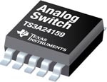
TS3A24159
0.3 Ohm Dual SPDT Analog Switch Dual-Channel 2:1 Multiplexer/Demultiplexer
Click for more information.
- Specified Break-Before-Make Switching
- Low ON-State Resistance (0.3 Ω Max)
- Low Charge Injection
- Excellent ON-State Resistance Matching
- Low Total Harmonic Distortion (THD)
- 1.65-V to 3.6-V Single-Supply Operation
- Control Inputs Are 1.8-V Logic Compatible
- Latch-Up Performance Exceeds 100 mA Per JESD 78, Class II
-
- ESD Performance Tested Per JESD 22
- 2000-V Human-Body Model (A114-B, Class II)
- 1000-V Charged-Device Model (C101)

Load Switches
TI's TPS229xx family of integrated load switches provides an easy solution to optimize the power consumption in a system by reducing the current leakages. These load switches are specially designed as a solution to the challenges that portable power management designers are facing. They integrate all the main features of a discrete load switch on a single die, providing maximum performance and flexibility to the end-user. Using integrated load switches is an easy way to implement a distributed power management architecture and to power down applications when they are not being used.
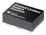
TPS22946
Ultra-Low Power, Low Input Voltage, Current Limited Load Switch
Click for more information.
- Ultra-Low Quiescent Current 1 µA (typ)
at VIN = 1.8 V
- Input Voltage Range: 1.62 V to 5.5 V
- Low ON-Resistance
- rON = 300 mΩ at VIN = 5.5 V
- rON = 400 mΩ at VIN = 3.3 V
- rON = 500 mΩ at VIN = 2.5 V
- rON = 600 mΩ at VIN = 1.8 V
- Selectable Minimum Current Limit:
155 mA, 70 mA, or 30 mA
- Integrated Inrush Current Timeout (8 ms)
- Shutdown Current: < 1 µA
- Thermal Shutdown
- Fault Blanking
- Auto Restart
- Over-Current Condition Timeout (Automatic Disable
for Permanent Over-Current)
- 1.8-V Compatible Control Input
- ESD Performance Tested Per JESD 22
- 6000-V Human-Body Model
(A114-B, Class II)
- Tiny WCSP Package 1.4mm &timews; 0.9 mm (YZP)
- APPLICATIONS
- Fingerprint Module Protection

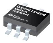
TPS22941
Low-Input Voltage 40mA Current Limited Load Switch with Shut-Off and Auto-Restart Features
Click for more information.
- Input Voltage Range: 1.62 V to 5.5 V
- Low ON resistance
- rON = 0.4 Ω at VIN = 5.5 V
- rON = 0.5 Ω at VIN = 3.3 V
- rON = 0.6 Ω at VIN = 2.5 V
- rON = 0.8 Ω at VIN = 1.8 V
- Minimum Current Limit: 40 mA or 100 mA
- Undervoltage Lockout
- Thermal Shutdown
- Shutdown Current < 1 µA
- Fast Current Limit Response Time
- Fault Blanking
- Auto Restart
- 1.8-V Compatible Control Input Thresholds
- ESD Performance Tested Per JESD 22
- 4000-V Human-Body Model
(A114-B, Class II)
- 1000-V Charged-Device Model (C101)
- Tiny SC-70 (DCK) Package
- APPLICATIONS
- Low-Current Sensor Protection

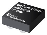
TPS22904
Ultra-Small Low-Input-Voltage Low rON Load Switch with Quick Output Discharge
Click for more information.
- Input Voltage: 1.1 V to 3.6 V
- Ultra-Low ON-State Resistance
- rON = 66 mΩ at VIN = 3.6 V
- rON = 75 mΩ at VIN = 2.5 V
- rON = 90 mΩ at VIN = 1.8 V
- rON = 135 mΩ at VIN = 1.2 V
- 500-mA Maximum Continuous Switch Current
- Quiescent Current < 1 µA
- Shutdown Current < 1 µA
- Low Control Input Threshold Enables Use of 1.2-V/1.8-V/2.5-V/3.3-V Logic
- Controlled Slew Rate (5 µs Max at 3.6 V)
- Quick Output Discharge (TPS22904 Only)
- ESD Performance Tested Per JESD 22
- 2000-V Human-Body Model
(A114-B, Class II)
- 1000-V Charged-Device Model (C101)
- 4-Terminal Wafer Chip-Scale Package (WCSP)
- 0.8 mm × 0.8 mm,
0.4-mm Pitch, 0.5-mm Height
- APPLICATIONS

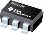
TPS22929D
Low Input Voltage, 1.8A Single Channel Load Switch with Controlled Turn-On
Click for more information.
- Integrated Single Load Switch
- Small SOT23-6 package
- Input Voltage Range: 1.4-V to 5.5-V
- Low ON-Resistance
- rON = 115-mΩ at VIN = 5-V
- rON = 115-mΩ at VIN = 3.3-V
- rON = 118-mΩ at VIN = 2.5-V
- rON = 129-mΩ at VIN = 1.5-V
- 1.8-A Continuous Switch Current (25C)
- Low Threshold Control Input
- Controlled Slew-rate Options
- Under-Voltage Lock Out
- Quick Output Discharge Transistor
- Reverse Current Protection

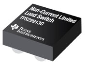
TPS22913C
Ultra-Small, Low rON, 2A Single Channel Load Switch with Controlled Turn-On
Click for more information.
- Integrated Single Load Switch
- Ultra Small CSP-4 Package 0.9mm × 0.9mm, 0.5mm Pitch
- Input Voltage Range: 1.4-V to 5.5-V
- Low ON-Resistance
- rON = 60-mΩ at VIN = 5-V
- rON = 61-mΩ at VIN = 3.3-V
- rON = 74-mΩ at VIN = 1.8-V
- rON = 84-mΩ at VIN = 1.5-V
- 2-A Maximum Continuous Switch Current
- Low Threshold Control Input
- Controlled Slew-rate Options
- Under-Voltage Lock Out
- Quick Output Discharge Transistor
- Reverse Current Protection

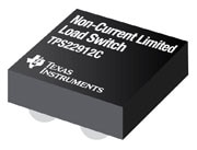
TPS22912C
Low Input Voltage, 2A Single Channel Load Switch with Controlled Turn-On
Click for more information.
- Integrated Single Load Switch
- Ultra Small CSP-4 Package 0.9mm × 0.9mm, 0.5mm Pitch
- Input Voltage Range: 1.4-V to 5.5-V
- Low ON-Resistance
- rON = 60-mΩ at VIN = 5-V
- rON = 61-mΩ at VIN = 3.3-V
- rON = 74-mΩ at VIN = 1.8-V
- rON = 84-mΩ at VIN = 1.5-V
- 2-A Maximum Continuous Switch Current
- Low Threshold Control Input
- Controlled Slew-rate Options
- Under-Voltage Lock Out
- Reverse Current Protection

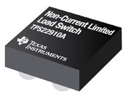
TPS22910A
Ultra-Small, Low rON, 2A Single Channel Load Switch with Controlled Turn-On
Click for more information.
- Integrated Single Load Switch
- Ultra Small CSP-4 Package 0.9mm × 0.9mm, 0.5mm Pitch
- Input Voltage Range: 1.4-V to 5.5-V
- Low ON-Resistance
- rON = 60-mΩ at VIN = 5-V
- rON = 61-mΩ at VIN = 3.3-V
- rON = 74-mΩ at VIN = 1.8-V
- rON = 84-mΩ at VIN = 1.5-V
- 2-A Maximum Continuous Switch Current
- Low Threshold Control Input
- Controlled Slew-rate Options
- Under-Voltage Lock Out
- Reverse Current Protection

I2C
As circuits become more complex with many peripheral connections, a method is needed to simplify designs and reduce costs. By limiting the number of printed circuit board (PCB) traces and lowering general purpose input and output (GPIO) usage on the microprocessor, the I2C bus met this requirement. Texas Instruments I/O expanders, multiplexers, buffers and repeaters can help system designers achieve effective subsystem communications and interfacing using proven I²C devices. The inter-integrated circuit I²C bus consists of two active wires; the bidirectional serial data (SDA) line and the bidirectional serial clock (SCL) line. TI's I²C portfolio includes TCA, PCA, and PCF technologies.
TCA5405
Low Voltage 5-Bit Self-Timed, Single-Wire Output Expander
Click for more information.
- Operating Power-Supply Voltage Range of 1.65 V to 3.6 V
- Five Independent Push-Pull Outputs
- Single Input (DIN) Controls State of All Outputs
- High-Current Drive Outputs Maximum Capability for Directly Driving LEDs
- Latch-Up Performance Exceeds 100 mA Per JESD 78, Class II

TCA6416A
Low-Voltage 16-Bit I2C and SMBus I/O Expander
Click for more information.
- Operating Power-Supply Voltage Range of 1.65 V to 5.5 V
- I2C to Parallel Port Expander
- Low Standby Current Consumption of 3 µA
- Schmitt-Trigger Action Allows Slow Input Transition and Better Switching Noise Immunity at the SCL and SDA Inputs

PCA9306
Dual Bi-Directional I2C-Bus and SMBus Voltage Level-Translator
Click for more information.
- 2-Bit Bidirectional Translator for SDA and SCL Lines
in Mixed-Mode I2C Applications
- I2C and SMBus Compatible
- Less Than 1.5-ns Maximum Propagation Delay to Accommodate
Standard-Mode and Fast-Mode I2C Devices and Multiple Masters
- Allows Voltage-Level Translator Between
- 1.2-V VREF1 and 1.8-V, 2.5-V, 3.3-V,
or 5-V VREF2
- 1.8-V VREF1 and 2.5-V, 3.3-V, or 5-V VREF2
- 2.5-V VREF1 and 3.3-V or 5-V VREF2
- 3.3-V VREF1 and 5-V VREF2
- Provides Bidirectional Voltage Translation With No Direction Pin
- Low 3.5-Ω ON-State Connection Between Input and Output Ports
Provides Less Signal Distortion
- Open-Drain I2C I/O Ports (SCL1, SDA1, SCL2, and SDA2)
- 5-V Tolerant I2C I/O Ports to Support Mixed-Mode Signal Operation
- High-Impedance SCL1, SDA1, SCL2, and SDA2 Pins for EN = Low
- Lock-Up-Free Operation for Isolation When EN = Low
- Flow-Through Pinout for Ease of Printed Circuit Board Trace Routing
- Latch-Up Performance Exceeds 100 mA Per JESD 78, Class II
- ESD Protection Exceeds JESD 22
- 2000-V Human-Body Model (A114-A)
- 200-V Machine Model (A115-A)
- 1000-V Charged-Device Model (C101)

TCA6408A
Low-Voltage 8-Bit I2C and SMBus I/O Expander
Click for more information.
- Operating Power-Supply Voltage Range of
1.65 V to 5.5 V
- Allows Bidirectional Voltage-Level Translation and
GPIO Expansion Between
- 1.8-V SCL/SDA and 1.8-V, 2.5-V,
3.3-V, or 5-V P Port
- 2.5-V SCL/SDA and 1.8-V, 2.5-V,
3.3-V, or 5-V P Port
- 3.3-V SCL/SDA and 1.8-V, 2.5-V,
3.3-V, or 5-V P Port
- 5-V SCL/SDA and 1.8-V, 2.5-V,
3.3-V, or 5-V P Port
- I2C to Parallel Port Expander
- Low Standby Current Consumption of 1 µA
- Schmitt-Trigger Action Allows Slow Input Transition and
Better Switching Noise Immunity at the SCL and SDA Inputs
- Vhys = 0.18 V Typ at 1.8 V
- Vhys = 0.25 V Typ at 2.5 V
- Vhys = 0.33 V Typ at 3.3 V
- Vhys = 0.5 V Typ at 5 V
- 5-V Tolerant I/O Ports
- Active-Low Reset (RESET) Input
- Open-Drain Active-Low Interrupt (INT) Output
- 400-kHz Fast I2C Bus
- Input/Output Configuration Register
- Polarity Inversion Register
- Internal Power-On Reset

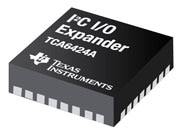
TCA6424A
Low-Voltage 24-Bit I2C and SMBus I/O Expander
Click for more information.
- Operating Power-Supply Voltage Range of 1.65 V to 5.5 V
- Allows Bidirectional Voltage-Level Translation and GPIO Expansion Between:
- 1.8-V SCL/SDA and
1.8-V, 2.5-V, 3.3-V, or 5-V P Port
- 2.5-V SCL/SDA and
1.8-V, 2.5-V, 3.3-V, or 5-V P Port
- 3.3-V SCL/SDA and
1.8-V, 2.5-V, 3.3-V, or 5-V P Port
- 5-V SCL/SDA and
1.8-V, 2.5-V, 3.3-V, or 5-V P Port
- I2C to Parallel Port Expander
- Low Standby Current Consumption of 1 µA
- Schmitt-Trigger Action Allows Slow Input Transition and
Better Switching Noise Immunity at the SCL and SDA Inputs
- Vhys = 0.18 V Typ at 1.8 V
- Vhys = 0.25 V Typ at 2.5 V
- Vhys = 0.33 V Typ at 3.3 V
- Vhys = 0.5 V Typ at 5 V
- 5-V Tolerant I/O Ports
- Active-Low Reset Input (RESET)
- Open-Drain Active-Low Interrupt Output (INT)
- 400-kHz Fast I2C Bus
- Input/Output Configuration Register
- Polarity Inversion Register
- Internal Power-On Reset

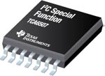
TCA6507
Low-Voltage 7-Bit I2C and SMBus LED Driver With Intensity Control and Shutdown
Click for more information.
- Seven LED Driver Outputs: On, Off, Blinking, Fading at Programmable Rates
- Open-Drain Outputs Directly Drive LEDs to 40 mA Max
- Can Be Configured Into Two Independent Banks of LED Drivers
- Widely Programmable Blink Rates, Fade-On and Fade-Off Rates and Maximum Intensity
- LED Intensity Set Using Pulse Width Modulation (PWM)
- Outputs Not Used as LED Drivers Can Be Used as Regular General-Purpose Open-Drain Outputs
- 16 Steps of Maximum Intensity Control from Fully-Off to Fully-On States
- 256 Intensity Levels During Fade-On or Fade-Off for Smooth Perceived Transition
- Operating Power-Supply Voltage Range of 1.65 V to 3.6 V
- EVM Available
- Schmitt-Trigger Action Allows Slow Input Transition and Better Switching Noise Immunity at the Inputs
- Vhys = 0.18 V Typ at 1.8 V
- Vhys = 0.25 V Typ at 2.5 V
- Vhys = 0.33 V Typ at 3.3 V
- 5.5-V Tolerant Open-Drain Outputs
- Low Standby Current with Shutdown Capability for Additional Power Savings
- Internal Power-On Reset
- Internal Oscillator Requires No External Components
- Programmed Through I2C Bus Interface Logic Compatible With SMBus
- 400-kHz Fast I2C Bus


TCA9555
Remote 16-Bit I2C And SMBus I/O Expander With Interrupt Output And Configuration Registers
Click for more information.
- Low Standby-Current Consumption of 3 µA Max
- I2C to Parallel Port Expander
- Open-Drain Active-Low Interrupt Output
- 5-V Tolerant I/O Ports
- Compatible With Most Microcontrollers
- 400-kHz Fast I2C Bus
- Address by Three Hardware Address Pins
for Use of up to Eight Devices
- Polarity Inversion Register
- Latched Outputs With High-Current Drive
Capability for Directly Driving LEDs
- Latch-Up Performance Exceeds 100 mA
Per JESD 78, Class II
- ESD Protection Exceeds JESD 22
- 2000-V Human-Body Model (A114-A)
- 200-V Machine Model (A115-A)
- 1000-V Charged-Device Model (C101)

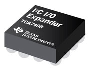
TCA7408
Low-voltage 8-bit I2C I/O Expander with Interrupt Output Reset I/O Direction Registers
Click for more information.
- Operating Power-Supply Voltage Range of 1.65V to 3.6V
- Allows Bidirectional Voltage-Level Translation and GPIO Expansion Between:
- 1.8V SCL/SDA and 1.8V, 2.5V, 3.3V GPIO port
- 2.5V SCL/SDA and 1.8V, 2.5V, 3.3V GPIO port
- 3.3V SCL/SDA and 1.8V, 2.5V, 3.3V GPIO port
- 5V SCL/SDA and 1.8V, 2.5V, 3.3V GPIO port
- Standby Current Consumption of <2 µA at 1.8V
- Active Current Consumption of:
- <2 µA at 1.8V 100 kHz clock
- <5 µA at 1.8V 400 kHz clock
- 100-kHz, 400-kHz Fast Mode
- Internal Power-On-Reset and Watchdog Timer
- Fail safe I2C, INT, and RESET lines
- Noise Filter on SCL/SDA and Inputs
- Schmitt-Trigger Action Allows Slow Input Transition and Better Switching Noise Immunity at the SCL and SDA Inputs
- Vhys = 0.18V Typ at 1.8V
- Vhys = 0.25V Typ at 2.5V
- Vhys = 0.33V Typ at 3.3V
- Active-Low Reset (RESET) Input
- Open-Drain Active-Low Interrupt (INT) Output

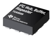
TCA9509
Level Translating I2C Bus Repeater
Click for more information.
- Two-Channel Bidirectional Buffer
- I2C Bus and SMBus Compatible
- Operating Supply Voltage Range of
2.7 V to 5.5 V on B side
- Operating Voltage Range of 0.9 V to VCCB – 1V on A Side
- Voltage-Level Translation From
0.9 V to (VCCB - 1V) and 2.7 V to 5.5 V
- Active-High Repeater-Enable Input
- Requires no external pull-up resistors on lower-voltage port-A
- Open-Drain I2C I/O
- 5.5-V Tolerant I2C and Enable Input Support Mixed-Mode Signal Operation
- Lockup-Free Operation
- Accommodates Standard Mode and Fast Mode I2C Devices and Multiple Masters
- Supports Arbitration and Clock Stretching Across Repeater
- Powered-Off High-Impedance I2C bus pins
- Supports 400-kHz Fast I2C Bus operating speeds
- Available in
- 1.6mm x 1.6mm, 0.4mm height, 0.5mm pitch QFN pkg
- 3mm x 3mm industry standard MSOP pkg
- Latch-Up Performance Exceeds 100 mA Per JESD 78, Class II
- ESD Protection Exceeds JESD 22
- 2000-V Human-Body Model (A114-A)

Translators
The ability to mix, match and support the simultaneous use of different operating supply voltage levels on the same circuit board has led to the need for voltage-level translation. Voltage-level translators or level-shifters address the challenges posed by simultaneous use of different supply-voltage levels on the same circuit board. Texas Instruments offers the industry's broadest level-translation portfolio to meet all your level shifter needs.
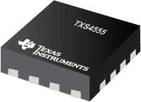
TXS4555
A complete SIM Card Solution for Interfacing Wireless Baseband Processors
Click for more information.
- Level Translator
- VCC Range of 1.65 V to 3.3 V
- VBATT Range from 2.3 to 5.5V
- Low-Dropout (LDO) Regulator
- 50-mA LDO Regulator With Enable
- 1.8-V or 2.95-V Selectable Output Voltage
- 2.3-V to 5.5-V Input Voltage Range
- Very Low Dropout: 100mV (Max) at 50mA

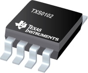
TXS0102
2-Bit Bidirectional Voltage-Level Translator for Open-Drain Application
Click for more information.
- No Direction-Control Signal Needed
- Max Data Rates
- 24 Mbps (Push Pull)
- 2 Mbps (Open Drain)
- Available in the Texas Instruments NanoFree™ Package
- 1.65 V to 3.6 V on A port and 2.3 V to 5.5 V on B port (VCCA ≤ VCCB)

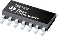
TXB0104
4-Bit Bidirectional Voltage-Level Translator with Auto Direction Sensing and +/-15 kV ESD Protect
Click for more information.
- 1.2 V to 3.6 V on A Port and 1.65 V to 5.5 V on
B Port (VCCA ≤ VCCB)
- VCC Isolation Feature – If Either
VCC Input Is at GND, All Outputs Are in
the High-Impedance State
- OE Input Circuit Referenced to VCCA
- Low Power Consumption, 5-µA Max ICC
- Ioff Supports Partial-Power-Down Mode Operation
- Latch-Up Performance Exceeds 100 mA Per JESD 78, Class II
- ESD Protection Exceeds JESD 22
- A Port
- 2500-V Human-Body Model (A114-B)
- 1500-V Charged-Device Model (C101)
- B Port
- ±15-kV Human-Body Model (A114-B)
- 1500-V Charged-Device Model (C101)


TXS0104E
4-Bit Bidirectional Voltage-Level Translator for Open-Drain Applications
Click for more information.
- No Direction-Control Signal Needed
- Max Data Rates
- 24 Mbps (Push Pull)
- 2 Mbps (Open Drain)
- Available in the Texas Instruments NanoFree Package
- 1.65 V to 3.6 V on A port and 2.3 V to 5.5 V on B port (VCCA ≤ VCCB)
- No Power-Supply Sequencing Required – VCCA or VCCB Can Be Ramped First
- Latch-Up Performance Exceeds 100 mA Per JESD 78, Class II
- ESD Protection Exceeds JESD 22
- A Port2000-V Human-Body Model (A114-B)200-V Machine Model (A115-A)1000-V Charged-Device Model (C101)
- B Port15-kV Human-Body Model (A114-B)200-V Machine Model (A115-A)1000-V Charged-Device Model (C101)
- IEC 61000-4-2 ESD (B Port)
- ±8-kV Contact Discharge
- ±10-kV Air-Gap Discharge

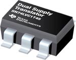
SN74LVC1T45
Single-Bit Dual-Supply Bus Transceiver with Configurable Voltage Translation and 3-State Outputs
Click for more information.
- Available in the Texas Instruments NanoFree™ Package
- Fully Configurable Dual-Rail Design Allows Each Port to
Operate Over the Full 1.65-V to 5.5-V Power-Supply Range
- VCC Isolation Feature – If Either VCC Input Is at GND,
Both Ports Are in the High-Impedance State
- DIR Input Circuit Referenced to VCCA
- Low Power Consumption, 4-µA Max ICC
- ±24-mA Output Drive at 3.3 V
- Ioff Supports Partial-Power-Down Mode Operation
- Max Data Rates
- 420 Mbps (3.3-V to 5-V Translation)
- 210 Mbps (Translate to 3.3 V)
- 140 Mbps (Translate to 2.5 V)
- 75 Mbps (Translate to 1.8 V)
- Latch-Up Performance Exceeds 100 mA Per JESD 78, Class II
- ESD Protection Exceeds JESD 22
- 2000-V Human-Body Model (A114-A)
- 200-V Machine Model (A115-A)
- 1000-V Charged-Device Model (C101)

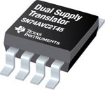
SN74AVC2T45
Dual-Bit Dual-Supply Bus Transceiver with Configurable Voltage Translation and 3-State Outputs
Click for more information.
- Available in the Texas Instruments NanoFree™ Package
- Control Inputs VIH/VIL Levels Are Referenced to VCCA Voltage
- Fully Configurable Dual-Rail Design Allows Each Port to Operate Over the Full 1.2-V to 3.6-V Power-Supply Range
- I/Os Are 4.6-V Tolerant
- Ioff Supports Partial-Power-Down Mode Operation
- Max Data Rates
- 500 Mbps (1.8-V to 3.3-V Translation)
- 320 Mbps (< 1.8-V to 3.3-V Translation)
- 320 Mbps (Translate to 2.5 V or 1.8 V)
- 280 Mbps (Translate to 1.5 V)
- 240 Mbps (Translate to 1.2 V)
- Latch-Up Performance Exceeds 100 mA Per JESD 78, Class II
- ESD Protection Exceeds JESD 22
- 8000-V Human-Body Model (A114-A)
- 200-V Machine Model (A115-A)
- 1000-V Charged-Device Model (C101)

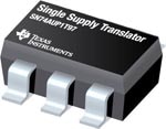
SN74AUP1T97
Single-Supply Voltage Translator
Click for more information.
- Available in the Texas Instruments NanoStar™ Packages
- Single-Supply Voltage Translator
- 1.8 V to 3.3 V (at VCC = 3.3 V)
- 2.5 V to 3.3 V (at VCC = 3.3 V)
- 1.8 V to 2.5 V (at VCC = 2.5 V)
- 3.3 V to 2.5 V (at VCC = 2.5 V)
- Nine Configurable Gate Logic Functions
- Schmitt-Trigger Inputs Reject Input Noise and Provide
Better Output Signal Integrity
- Ioff Supports Partial-Power-Down Mode With
Low Leakage Current (0.5 µA)
- Very Low Static and Dynamic Power Consumption
- Pb-Free Packages Available: SON (DRY or DSF),
SOT-23 (DBV), SC-70 (DCK), and NanoStar WCSP
- Latch-Up Performance Exceeds 100 mA Per JESD 78, Class II
- ESD Performance Tested Per JESD 22
- 2000-V Human-Body Model
(A114-B, Class II)
- 1000-V Charged-Device Model (C101)
- Related Devices: SN74AUP1T98, SN74AUP1T57, and SN74AUP1T58

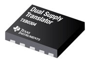
TXB0304
4-bit Bidirectional Auto-direction Sensing Translator with Fully Symmetric 0.9V to 3.6V Range
Click for more information.
- Fully Symmetric Supply Voltages. 0.9 V to 3.6 V on A Port and 0.9 V to 3.6 V
- VCC Isolation Feature – If Either VCC Input Is at GND,
All Outputs Are in the High-Impedance State
- OE Input Circuit Referenced to VCCA
- Low Power Consumption, 5-µA Max (ICCA or ICCB)
- Ioff Supports Partial-Power-Down Mode Operation
- Latch-Up Performance Exceeds 100 mA Per JESD 78, Class II
- ESD Protection Exceeds JESD 22
- 8000-V Human-Body Model (A114-B)
- 1000-V Charged-Device Model (C101)

|
Guides
Featured Videos
Product Training Modules
|


 1µA at VOL, VOH
 )
)